Professor Aris Christou
Department of Materials Science and Engineering | Department of Mechanical Engineering
A. James Clark School of Engineering | Universty of Maryland
Laboratory for Reliable Electronics
The Laboratory for Reliable Nanoelectronics is an advanced facility for semiconductor device process development, test structure design for reliability and Reliability measurements at the University of Maryland. It includes a broad variety of advanced materials processes and supporting processes for fabricating of devices and reliability test structures.
To support these activities, the facility houses a wide variety of equipment for wet and dry semiconductor processes as well as analytical tools. It includes a UHV system for Atomic Layer Deposition and a MAS 400 mask aligner for high resolution contact lithography, an e-beam metallization chamber, sol-gel and photoresist spinners, annealing and oxidation furnaces, several optical microscopes as well as a variety of chemical gas sensors (RGAs, FTIR, acoustic sensors) for in-situ process diagnostics.
equipment within the facility:
UHV Atomic Layer Deposition system
high density plasma etch cluster tool, Alliance 9400
MAS 400 IR/VIS mask aligner
4 point probe station for sheet resistance measurements
Residual gas analyzer, Inficon 300 amu
Residual gas analyzer, Inficon 200 amu
Gas phase acoustic sensor, Inficon Composer
FTIR compact spectrometer, Inficon
E-beam metal evaporator, CV8 Airo Temescal
8" sol-gel spincoater,
SP 100 Bidtec controller
8" photoresist spincoater, SP 100 Bidtec
Programmable hot plate, 400C; for sol-gel and photoresist
Programmable furnace, Vulcan 3-550,
Oven, Blue M, Electric Gal. Signal L.
Oven, Lindberg, Electric Gal. Signal L.
Oxidation tubular furnace, Blue M
microbalance, 1/10000g
Microscope, Ferroscope L.
Microscope, Optiphot POL, Nikon
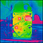
Barnes Infrared Microscope
Scanning Acoustic Microscope


